
Solved
32F417 and RDP2: OTP (512 bytes) and SRAM execution
This
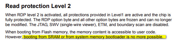
suggests that one cannot execute code from SRAM. Is that really correct?
Also there is ambiguity on whether the OTP area (512 bytes plus the control block) is readable in RDP2. Why say "512 bytes" and not just all-OTP?

The OTP area must remain usable under RDP2 and readable by internal code, but not accessible externally (with a debugger).
Above is from